PCB design
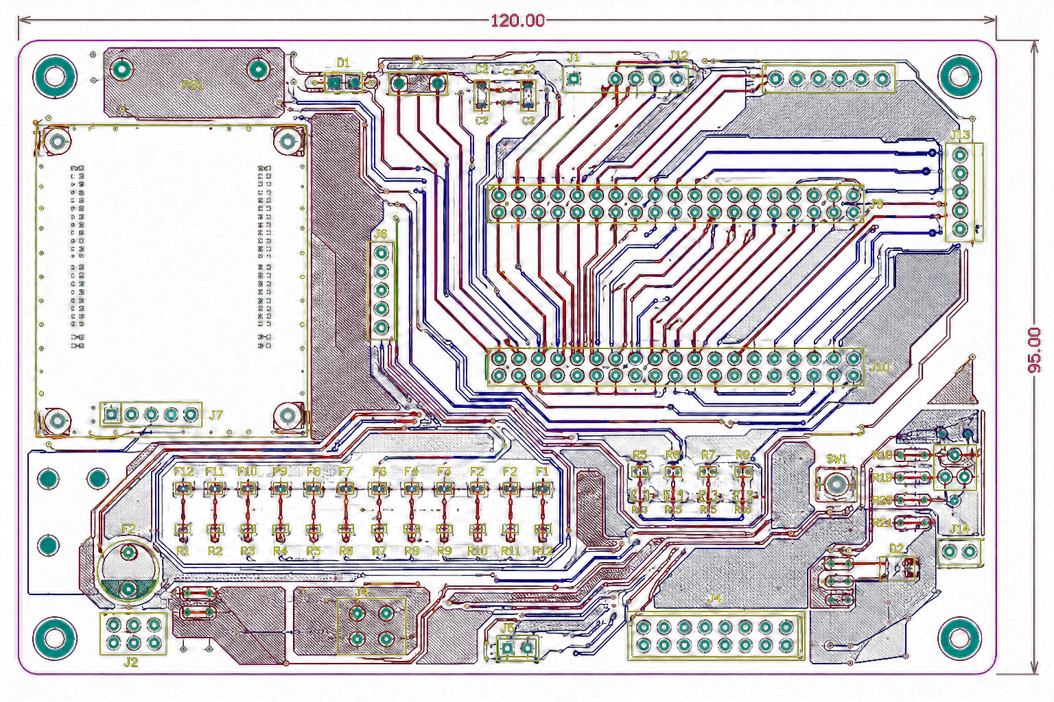
Layout is where the schematic becomes a real product
A design that simulates well can still fail EMC, cost too much to assemble, or be impossible to rework. We lay out boards with the fabricator, the compliance lab and the service engineer all in mind.
Services
What PCB design covers here
Not just track routing. The decisions that determine whether a board works, passes, and can be built at volume.
Schematic capture
Stackup and impedance
High-speed routing
Mixed-signal and power
EMC-aware layout
Design for manufacture
Capability
Complexity we take on
If your board sits outside this, tell us anyway — the honest answer is sometimes that a different partner suits you better.
Construction
- Single-sided through to high layer-count boards
- HDI with blind, buried and microvias
- Fine-pitch BGA fanout and escape routing
- Rigid and rigid-flex construction
Signal integrity
- Controlled impedance, single-ended and differential
- DDR and memory interface routing
- USB, Ethernet, PCIe and MIPI
- RF and antenna keep-out planning
Deliverables
- Fabrication drawings and Gerber or ODB++
- Assembly drawings and pick-and-place data
- Bill of materials with sourcing notes
- Stackup specification and impedance report
Process
How a layout runs
The middle stages are where clients have most influence, and where changes are still cheap.
- 01
Constraints first
Before a single track is placed we agree the stackup, the impedance targets, the mechanical envelope and the manufacturing capability we are designing to.
- 02
Placement review
Component placement is where a board is won or lost. You see it, and sign it off, before routing begins — moving a connector later is expensive.
- 03
Route and verify
Routing against the agreed constraint set, then design rule checks, netlist verification against the schematic, and a 3D clearance check against the enclosure.
- 04
Release and support
Manufacturing data released to your fabricator or ours, then we stay available through the fabrication queries that always arrive.
Worth knowing
Why placement gets a sign-off
Most of a board's cost, its thermal behaviour, its EMC performance and its serviceability are fixed the moment components are placed. Routing afterwards can only work within those decisions.
So placement is a checkpoint, not an internal step. You see the layout before routing starts, with the reasoning for each cluster — why the regulator sits where it does, why the connector faces that edge, what the keep-outs are protecting. Objections at that stage cost an afternoon. The same objection after routing costs a re-spin.
Evidence
Boards we have laid out
Projects where the layout carried real constraints — mains power, isolation, or a tightly specified output stage.
Turn-key IoT platform for trackside monitoring and data logging
Connected LED signal marker board for railway applications
Turn-key design of a precision 56 kHz loop signal generator
Related
Layout rarely arrives alone
Most PCB work here sits inside a wider engagement. It does not have to.
Send us a schematic
Or a block diagram and a rough mechanical envelope. We will come back with a stackup proposal, the constraints we would design to, and an honest view of the risky parts.